Perforation positioning
Standard SMT applications such as QFP or BGA device screen printing, the application of solder paste in the center of the pad, but the printed wafer is less so, but the entire pad is printed completely, so that the amount of paste is sufficient to form a height Distribution of effective solder paste bumps. In very small spaces, it may be difficult to place the perforations symmetrically with the pads and leave enough space (ie, a minimum of 3 mils) between adjacent perforations to prevent bridging defects. In this case, it is recommended that the solder paste should cover at least 50% of the solder pad so that the solder paste is properly withdrawn and completely coalesced on the pad. In addition, in order to make the withdrawal process ideal, the center of the perforation (not the end) is preferably offset from the pad, as shown in FIG. 4 .
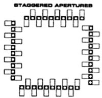
Figure 4: In both cases, the elongated elliptical perforation offset pads are placed in both cases. When printing through perforations B, the solder paste is pulled back to the pad during reflow.
For a closely spaced pad with a single row perimeter arrangement, large scale coating to avoid bridging can be a challenge. Wafers designed for wire bonding of chip electrical interconnects typically have this configuration. In these cases, the perforations can be made into elongated elongated ellipses or rectangular geometries and arranged in a staggered pattern to separate adjacent solder paste coatings.
Figure 5: For single-row pad configurations, an effective way to apply a large amount of solder paste to the pad and reduce the bridging risk is to stagger the perforations.
An example of this approach is shown in Figure 5. If space is sufficient, this staggered arrangement can also be applied to multiple rows of pad layouts. Solder pastes that do not have any non-passivating metal must be used for the pads in the vicinity of the die sawing channel. It is important to note that perforations cannot be placed on other exposed metal properties (eg, fiducials, marks, or trademarks) that do not accept solder paste. These features may have serious effects on the effectiveness of such bumping methods. Impact, and bring great challenges for perforated placement process. In addition, it may be difficult to find enough space to fit the perforations at the corner pad pads. Since the maximum limitation of the perforation characteristics comes from these aspects, it is recommended to start the screen design process based on these conditions to avoid possible catastrophic problems in the downstream process.
in conclusion
Screen printing wafer bumping technology is a low-cost solution that can be used for production and can replace conventional process technologies such as evaporation or electroplating. However, as the number of I/Os increases and the spacing decreases, the use of stencils to print solder paste on these solder joints is becoming more and more challenging, and, for matching materials (such as solder pastes, nets) Plates, etc.) and process design standards have also been greatly improved. Therefore, people continue to carry out research in order to better understand these details, so as to achieve the purpose of further improving the screen printing wafer bumping process.
Dog Repeller,Pest Repeller,Pest Control
Mosquito Trap,Animal Repeller Co., Ltd. , http://www.chinapestrepeller.com